Fundamentals and Practices of Sensing Technologies
by Dr.
Keiji Taniguchi, Hon. Professor of
Xi’ an
Dr. Masahiro Ueda, Honorary
Professor, Faculty of Education and Regional Studies
Dr. Ningfeng Zeng, an
Engineer of Sysmex Corporation
(A Global Medical
Instrument Corporation),
Dr. Kazuhiko Ishikawa,
Assistant Professor
Faculty of Education and
Regional Studies,
[Editor’s
Note: This paper is presented as Part V of a series from the new book
“Fundamentals and Practices of Sensing Technologies”; subsequent chapters will
be featured in upcoming issues of this Journal.]
Chapter 2 (Section II): Overviews of Classical
Transducers
2.6 Optical Sensors Using Photo
Devices
Photo-devices
such as photodiodes are used as sensors for
converting optical flux into circuit current.
2.6.1 Optical Sensing
Devices Using Photodiodes (10)
We deal with typical photodiodes,
since many types of photodiodes exists.
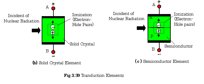
A. General P -N Junction Photodiodes
The p-n junction photodiodes are classified into two categories: one is
the depletion layer type and another is the avalanche type.
Figure 2.26(a) shows the p-n junction of a photodiode. The light is illuminated at the vicinity of the junction in
the photodiode, and the following diode
current ![]() is caused:
is caused:
![]()
![]() (2.22)
(2.22)
, where ![]() is a dark current due
to the thermal carriers, in other words,
electrons and holes (See comment 2.1),
is a dark current due
to the thermal carriers, in other words,
electrons and holes (See comment 2.1), ![]() is a constant,
is a constant, ![]() is a luminous flux on the surface, and
is a luminous flux on the surface, and ![]() is the wavelength of
the light.
is the wavelength of
the light.
The output voltage ![]() of this circuit is,
then, expressed as follows (See Fig.2.26 (b)):
of this circuit is,
then, expressed as follows (See Fig.2.26 (b)):
![]() (2.23)
(2.23)
The dark current![]() is the most important factor for determining the sensitivity of the sensor, i.e., minimum detectable
current.
is the most important factor for determining the sensitivity of the sensor, i.e., minimum detectable
current.
B. P-I-N Junction Photodiodes
The p-i-n junction photodiode has higher electric field layer made of an intrinsic semiconductor i between p and n regions shown in Fig. 2.26(a).
The carriers generated in junction
regions are rapidly separated by the intrinsic layer which make possible faster
frequency response, because such a
constitution can minimize the generation of slow carriers.
C . Avalanche Photodiodes
An avalanche photodiode operates at higher reverse biased voltage that is little smaller than a break down voltage. In this case, carriers in the depletion layer are accelerated, and then create more and more carriers by repeated collisions. There are, then, a lot of carriers in this layer by the avalanche multiplication effect which can give rise to a current gain of approximately
Figure 2.27 shows a structural model of photo multipliers. These are the most sensitive light sensing devices. The operation of these devices is as follows:
(1) Photoelectrons
![]() flow through the photo
cathode toward dynode
flow through the photo
cathode toward dynode ![]() due to the light
irradiation on this photo cathode.
due to the light
irradiation on this photo cathode.
(2) These
photoelectrons,
dynode![]() emit secondary electrons
emit secondary electrons ![]() ,
, ![]() toward dynode
toward dynode ![]() . Such operations are
repeated between dynodes
. Such operations are
repeated between dynodes ![]() and
and ![]() ,
,
(![]() ).
).
(3) The
multiplied photoelectrons on the dynode ![]() are, finally,
collected on an anode. The anode current
are, finally,
collected on an anode. The anode current ![]() caused by these
electrons is expressed as follows:
caused by these
electrons is expressed as follows:
![]() ,
, ![]() (2.24)
(2.24)
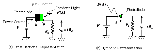
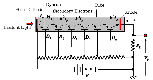
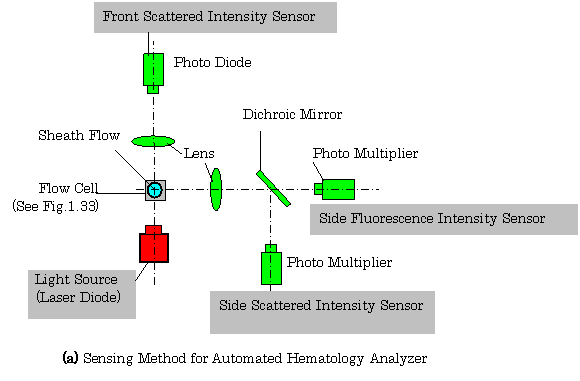
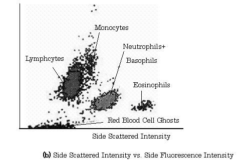
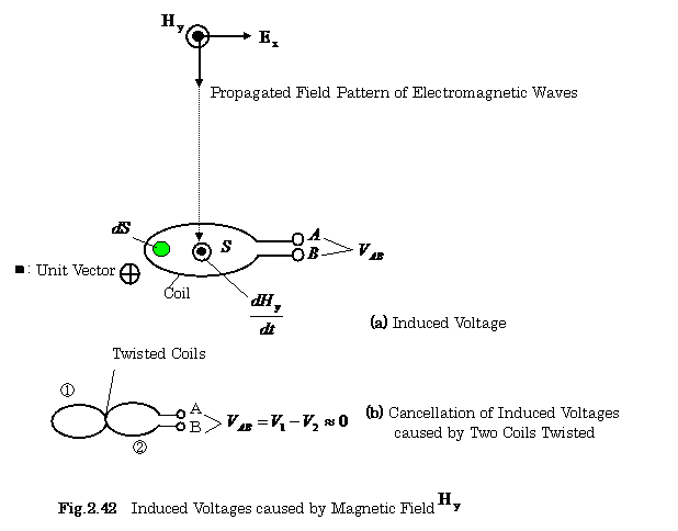
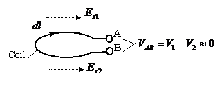
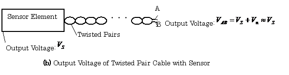
【Example 2.12】(7), (8) Figure 2.28(a) shows the configuration of a sensor for automated hematology analyzer using a photo-diode and two photo-multipliers. In this figure, the mechanism of the generation of sheath flow is shown in Fig. 1.28.
![]()
-+
![]()
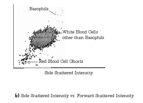
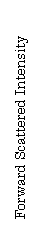
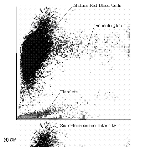
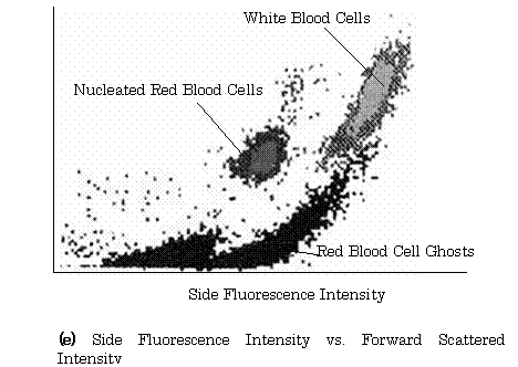
Fig.2.28 Sensing System of Automated Hematology Analyzer
and Measurement Results
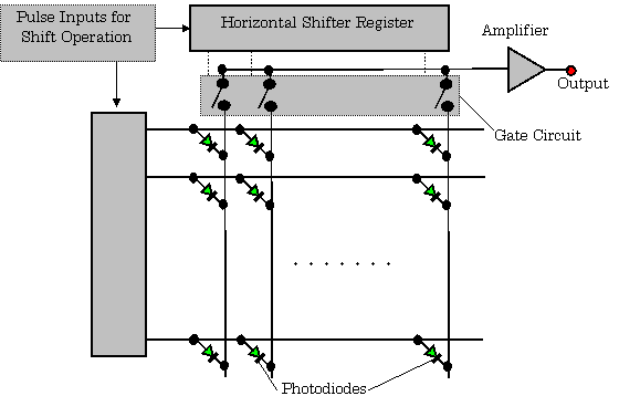
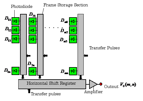
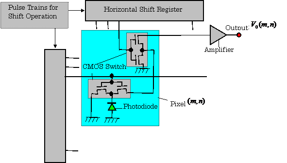
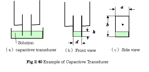
2.6.3 Image Sensors Constituted by Means of Photodiode Array (12)
![]()
![]()
![]()
These image data are serially read out from the output ![]() of an amplifier
of an amplifier
In this case, the numbers of pixels are ![]() . An optical low-pass filter fabricated
. An optical low-pass filter fabricated
![]()
![]()
![]()
![]()
![]()
![]()
![]()
![]()

![]()
【Example 2.13】
The block diagram of this system is shown in Fig.2.32.
The timing signals for synchronizing an image sensor, an A-D converter, and digital signal processor (DSP), are generated by a signal generator.
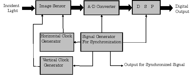
Fig.2.32 Constitution of Image Sensing System
2.7 Analog Signal Processing Circuits
2.7.1 Unbalanced Input Amplifiers
Figure 2.33 shows the typical circuits for unbalanced
amplifiers, where one of signal source lines is grounded.

The output voltages of these amplifiers are expressed as follows:
(1)Inverting amplifier ![]() (2.25)
(2.25)
(2) Non-inverting amplifier ![]() (2.26)
(2.26)
(3) Voltage follower ![]() (2.27)
(2.27)
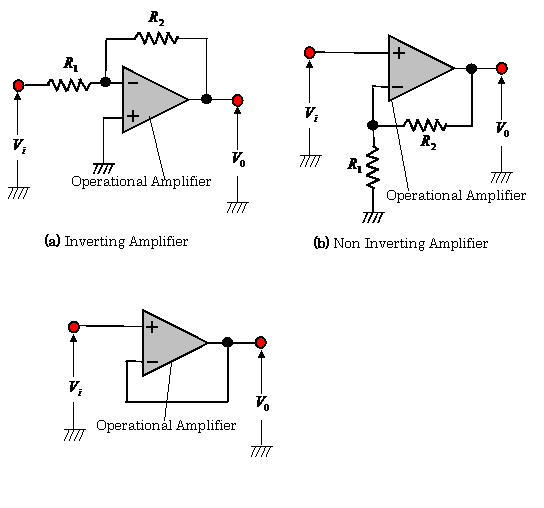
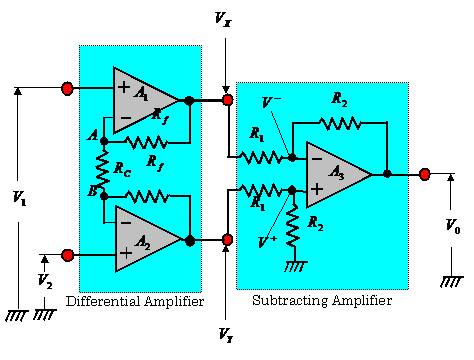
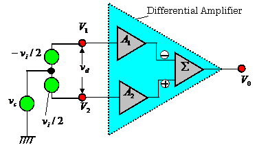
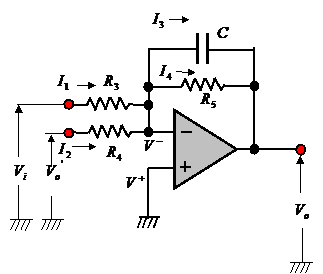
2.5.2 Typical Balanced Input Amplifier (11)
Figure.2.34 shows a typical balanced input amplifier circuit. This
circuit consists of two stages: an amplification
circuit and a subtraction circuit.
(1) The output
voltages of the differential amplifier are expressed as follows:
![]() ,
, ![]() (2.28)
(2.28)
(2) In the subtracting circuit of 2nd stage, the output voltage ![]() is expressed as
follows:
is expressed as
follows:
![]() (2.29)
(2.29)
where ![]() , and
, and ![]() are input voltages of the
differential amplifier.
are input voltages of the
differential amplifier.
(3) From Eqs.(2.28 ) and (2.29), the output voltage![]() of this circuit is expressed as follows:
of this circuit is expressed as follows:
![]() (2.30)
(2.30)
where
![]()
![]() and
and ![]() are the
input voltages of this amplifier.
are the
input voltages of this amplifier.
This circuit has the large common- mode rejection
ratio(CMRR
Differential gain/Common mode gain), and is useful for
reducing the common- mode noise induced in the
input signal.
The details of Fig.2.34 are described in the solution of Problem 2.2.

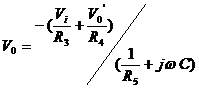
【Example 2.14】Figure 2.35 shows a
basic model of a differential amplifier.
In this figure, the equivalent
circuit of an input signal is described in Fig.2.35.
Find an output voltage ![]() , a differential mode gain
, a differential mode gain![]() , a common mode gain
, a common mode gain ![]() , and a common mode
rejection ratio (CMRR) which is defined as a ratio of the differential gain to the
common mode gain:
, and a common mode
rejection ratio (CMRR) which is defined as a ratio of the differential gain to the
common mode gain: ![]() in this amplifier.
in this amplifier.
【Solution】In this figure, we
can get the following relations:
![]() ,
, ![]() ,
, ![]()
![]()

From the relationships
described above , the output voltage
![]()
is expressed as follows:
![]()
![]()
Here, we define as:![]() ,
, ![]() , so the output
voltage
, so the output
voltage ![]() is expressed as follows:
is expressed as follows:
![]()
![]()
![]()
2.7.3 Small Signal Linear Rectifier (11)
Figure.2.36 shows a small signal linear rectifier circuit.
The output voltage ![]() of this circuit is
expressed as follows:
of this circuit is
expressed as follows:
![]() (2.31)
(2.31)
where ![]() ,
, ![]() .
.
The details of Fig.2.36 are described in the solution of Problem 2.3.
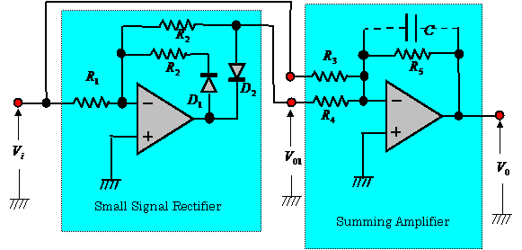
![]()
2.8 Application Examples for Measurements
2.8.1. Transducers or Sensors for Solid Mechanical Measurements(1 )
A. Position or Displacement
As a symbol of this value, we use here “![]() ”.
”.
(a) Position
This is the “scalar value” representing a special location of a point with respect to a reference point.
(b) Displacement
This is the “vector value” representing a change in position of a point with respect to a reference point.
( c ) Position or Displacement Transducers
(1)Strain-gage (See section 2.2 in this chapter), (2) Relactive transducer( See section 2.3 in this chapter) , (3) Capacitive transducer ( See section 2.4 in this chapter), (4) Piezoelectric transducer ( See section 2.5 in this chapter)
B. Speed or Velocity Definition
![]() , (
, (![]() is a time).
is a time).
(a) Speed: This is a scalar value.
(b) Velocity: This is a vector value.
C. Definitions for
Acceleration, Vibration and Shock
(a)
Linear acceleration
 , (
, ( is a time).
(b)
Angular acceleration
 , (
, ( is an angular frequency).
(c)
Mechanical vibration: Usually the vibratory acceleration is applied.
(d)
Shock: This is defined as a sudden non-periodic or transient excitation.
D. Principles of Measurements
for Acceleration, Vibration and Shock(1)
(A) Acceleration
A dynamical quantity like
acceleration is converted into a mechanical one. That is, a force is firstly converted into a
displacement and is secondary converted into a voltage signal by means of a
sensor such a VLDT (variable linear differential transformer). See section 2.3 in this
chapter.
Under a linear movement, a
velocity and an acceleration are expressed by the following equations as
the time rate of the change of displacement ![]() and velocity
and velocity![]() , respectively.
, respectively.
(1) Velocity: ![]() , (2) Acceleration:
, (2) Acceleration:![]()
where![]() is the time. Figure 2.37 shows the
sensing device for acceleration measurement. The sensor consists of a seismic mass
is the time. Figure 2.37 shows the
sensing device for acceleration measurement. The sensor consists of a seismic mass
![]() , a damper of damping factor
, a damper of damping factor ![]() , and a spring of spring-constant
, and a spring of spring-constant ![]() .
.
Acceleration sensor is also used for measuring the vibration and shock.
We consider here a motion of the mass when a
force ![]() is firstly applied
horizontally to
is firstly applied
horizontally to
a
sensor-case as shown in Fig. 2.37 (b), and then removed. The mass will be
returned to
its steady state position by the spring as
shown in Fig. 2.37 (a). A displacement of the
mass is converted into an electrical signal by
means of a transduction element such as
a LVDT. The equation of motion of the mass is
expressed as follows:
![]() (2.32)
(2.32)
where ![]() ,
,![]() is a unit step function( when
is a unit step function( when ![]() , then
, then ![]() ,
, ![]() , then
, then ![]() ). The acceleration is, then expressed as follows:
). The acceleration is, then expressed as follows:
![]() (2.33)
(2.33)
where  ,
, ,
, , and
, and will be described by Eqs.(6) and (9) in comment 2.2.
(B) Vibration and Shock
(1) A vibration can generally be
approximated by the sinusoidal function:
![]() (2.34)
(2.34)
where ![]() expresses the real
part of
expresses the real
part of ![]() .
.
(2) A shock can be approximated by a unit- step
function as follows:
![]() (2.35)
(2.35)
where ![]() is a pulse width of the shock wave.
is a pulse width of the shock wave.
【Comment 2.2】(13)
In Fig.2.33 (a), the displacement ![]() is expressed as
follows:
is expressed as
follows:
![]() (1)
(1)
where we put ![]() , and
, and ![]() , so this equation is rewritten as follows:
, so this equation is rewritten as follows:
![]() (2)
(2)
(1)Displacement:![]()
The displacement![]() is expressed as follows:
is expressed as follows:
![]() (3)
(3)
where![]() , and
, and ![]() express a transient
state displacement and a steady state displacement, respectively.
express a transient
state displacement and a steady state displacement, respectively.
(2)Steady State
Component in Displacement: ![]() (4)
(4)
(3)Transient State Component in Displacement:
The transient displacement![]() can be obtained from the following equation.
can be obtained from the following equation.
![]() (5)
(5)
Putting ![]() , we obtain
, we obtain ![]() ,
, ![]() .
.
By inserting these results into
Eq. (5), we can, then, get ![]() as follows:
as follows:
![]() ,
,
![]() ,
,
![]() (6)
(6)
For the case ![]() , the transient response is obtained as follows
, the transient response is obtained as follows
![]() (7)
(7)
From Eqs.(3), (4), (6), and (7),
finally, the displacement![]() is expressed as follows:
is expressed as follows:
![]() (8)
(8)
Two constants A1 and A2 of integration in
equation (8), can be determined by means of the initial conditions, such as ![]() , and
, and ![]() for
for ![]() ;
;
![]() ,
, ![]() .
.
The constants ![]() and
and ![]() are, then, determined
as follows:
are, then, determined
as follows:
![]() ,
, ![]() (9)
(9)
From Eq. (8), the acceleration can
be expressed as follows:
![]() (10)
(10)
【Example 2.15】Find the acceleration
and the displacement in the case of ![]() shown in Eq.(6) in comment (2.2).
shown in Eq.(6) in comment (2.2).
【Solution】
From Eqs. (3), (4),and![]() , the displacement
, the displacement![]() and the velocity
dx/dt are expressed as follows:
and the velocity
dx/dt are expressed as follows:
![]() (11)
(11)
![]() (12)
(12)
Using initial conditions of ![]() and
and ![]() , for t=0 in Eqs.(11) and( 12), the constants,
, for t=0 in Eqs.(11) and( 12), the constants, ![]() and
and ![]() can be obtained as
follows:
can be obtained as
follows:
![]() , and
, and ![]()
![]() ,and
,and ![]() (13)
(13)
The acceleration can, then be
expressed as follows:
![]() (14)
(14)
E. Force and Pressure (Force/Unit Area) Sensors
Strain gage force transducers are most widely used. The PZT force transducers are used for dynamic
compression force measurements. They are described in sections 2.2 and 2.5 of
this chapter.
2.8.2.
Transducers or Sensors for Fluid Mechanical Measurements
A. Liquid Level Transducers or
Sensors
For example, the capacitive
transducers and photo sensors described in sections 2.4 and 2.6 of this chapter
are used for these measurements.
B. Pressure Transducers or
Sensors
For example, these devices are
described in 2.8.1 E in this chapter.
C. Flow Sensors ( 4)
Figure 2.38 shows a differential
pressure sensing method for fluid flow measurement. A flow rate ![]() determined by the time
rate of fluid motion and a volume-metric flow
determined by the time
rate of fluid motion and a volume-metric flow ![]() for a circular pipe
shown in this figure, are expressed as follows:
for a circular pipe
shown in this figure, are expressed as follows:
![]() (2.36)
(2.36)
![]() (2.37)
(2.37)
where ![]() ,
, ![]() , and
, and![]() is the height (head) of fluid:
is the height (head) of fluid: ![]() .
.
![]()
2.8.3 Transducers for Thermal
Measurements(1)
Temperature
transducers or sensors are classified to two categories: one is surface transducers,
and another is immersion- probe transducers. These are described in sections
2.1 and 2.2 of this chapter.
2.8.4 Transducers or Sensors
for Acoustic Measurements
For example, these devices are
described in chapter 3 in this book.
2.8.5 Transducers or Sensors
for Optical Measurements
Photo conductive junction transducers and photo multiplier
tubes are described in section 2.6 of this chapter.
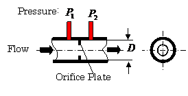
2.8.6 Transducers or Sensors for Nuclear Radiation Measurements(1)
Nuclear radiations are divided broadly
into two categories: one is the radiation with the emission of charged and
uncharged particles such as ![]() (protons) and
(protons) and ![]() (electrons) particles and neutrons, and another is
electromagnetic wave radiations such as x and gamma rays from the atomic
nuclei.
(electrons) particles and neutrons, and another is
electromagnetic wave radiations such as x and gamma rays from the atomic
nuclei.
These radiations can be measured
by means of the ionized transduction elements shown in Fig. 2.39. In this
figure, (a) shows a gas tube transduction element connected to an electrical
conversion circuit, (b) also shows a solid crystal transduction element, and
finally, ( c ) shows a semiconductor transduction element. In these
transduction elements, the ionizations are occurred due to the nuclear
radiation. As the results in this
circuit, the current ![]() shown in figure (a)
flows, and the output voltage
shown in figure (a)
flows, and the output voltage ![]() is obtained as:
is obtained as: ![]() .
.
【References】
(1) D. Christiansen: Electronics Engineers’ Handbook, 4th Edition, pp.13.1-13.50
IEEE Press (1997)
(2) R. C. Dorf: Electrical Engineering Hand Book, p.14,p.1156, pp.1088-1091, CRC Press (1993)
(3) P. Kantrowtts, G.Kousourou, L. Zucker: Electronic Measurements, pp.294-298,
Prentice Hall (1979)
(4) P.H. Garrett: Analog system for Microprocessors and Minicomputers, pp.1-40,
(5) L. K. Baxter: Capacitive Sensors (Design and Applications), pp 40-81,
IEEE Press (1997)
(6) Mitsubishi Electric Corp. Ltd, Triple A: Acceleration sensor(2005-October)
(7) K.Turuda, T.Tyji, T.Usui, S.Kitajima, A.Kihara, M.Murai, Y.Kasada, Q.Li,
Y.Yamada and S.Kamihira: Evaluation and Clinical Usefulness of the Automated Hematology Analizer, Sysmex XE-2100TM, Sysmex Journal International, Vol.19, No2 (Winter1999)
(8) Overview of Automated Hematology analyzer XE-2100TM, Product Development
Division, Sysmex Corporation, pp.76-84, Sysmex Journal, Vol.22, No1 (Spring 1999)
(9) H.Ozaki, K.Taniguchi: Sensors and Signal Processing (2nd Edition), pp.17-25,
Kyoritsu Pub.Co. Ltd. (1988), (In Japanese)
(10) H.Ozaki, Y.Kanata, K.Taniguchi, M.Yokoyama: Analog Electronic Circuits
(2nd Edition), pp.110-111, Kyoritu Pub.Co. Ltd. (1992), (In Japanese)
(11) K. Taniguchi (Edition): Fundamentals of Signal Processing, pp.72-76, Kyoritsu Pub.Co. Ltd. (2001), (In Japanese)
(12) Television Institute Edition: Television Image Information Engineering
Handbook, pp.156-163, Ohm Pub. Co. Ltd.(1990),(In Japanese)
(13) H. Ozaki : Transient Phenomena of Electrical Circuits(2nd Edition),pp.18-22,
Kyoritu Pub. Co. Ltd. (1982), (In Japanese)
【Problems and solutions】
2.1 In a capacitive transducer shown in Figure2.40, calculate
the following two values:
(1) Small change ![]() in the capacitance
in the capacitance![]()
(2) Ratio ![]() in a case of
in a case of ![]() , and
, and![]() .
.
【Solution】
(1):From Eq.(2.15),
![]() ,
, ![]() ,
, ![]()
(2):![]()
2.2 Derive Eqs.(2.28) and(2.29).
【solution】
(1)In the differential amplification circuit shown inFig.2.34, ![]() is the voltage between
point A and the ground, and
is the voltage between
point A and the ground, and ![]() is also the
voltage between point B and the ground. So, the following equations are
obtained.
is also the
voltage between point B and the ground. So, the following equations are
obtained.
![]() ,
,![]() ,
, ![]() ,
, ![]()
From these equations,![]() and
and ![]() are expressed as
follows:
are expressed as
follows:
![]() ,
, ![]()
(2) In subtraction circuit shown inFig.2.34,
the following equations are obtained.
![]() ,
, ![]()
From these equations,![]() is expressed as follows:
is expressed as follows:
![]()
(3) From the results obtained above, ![]() is expressed as
follows:
is expressed as
follows:
![]()
2.3 Derive
Eq.(2.31), where![]() ,
, ![]() .
.
【solution】
In Fig2.36,
(1) if ![]() , then
, then ![]() ,
, ![]() ,
, ![]() ,
,
From these equations, the output voltage is expressed as ![]() .
.
(2) if ![]() , then
, then ![]() ,
,![]() ,
, ![]() ,
,
where ![]() ,
, ![]() . From these
equations, the output voltage is expressed as
. From these
equations, the output voltage is expressed as ![]() .
.
From the results described above, the output voltage ![]() that is independent to
the polarity of the input voltage, is expressed as follows:
that is independent to
the polarity of the input voltage, is expressed as follows:
![]()
 2.4
Find the gain and the cut- off frequency of the circuit shown in Fig.2.41.
2.4
Find the gain and the cut- off frequency of the circuit shown in Fig.2.41.
Fig.2.41
(1) Gain:
In the figure, the following equations are obtained.
![]() ,
, ![]() ,
, ![]() ,
,
![]() ,
, ![]() ,
, ![]() ,
, ![]()
From these equations, the output voltage ![]() is expressed as
follows:
is expressed as
follows:
where ![]() .
.
In the case of ![]() ,
,![]() ,the gain
,the gain ![]() of this circuit is expressed as follows:
of this circuit is expressed as follows:
![]()
(2) Cut- off frequency:
From the equation , the cut- off frequency
 ![]() is expressed as follows:
is expressed as follows:
![]()
![]()
![]()
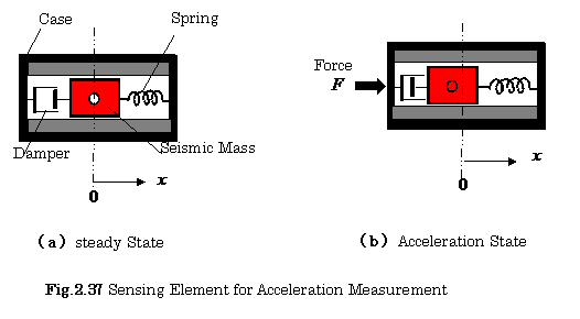
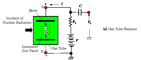
2.5 Explain the reason that a twisted-cable is used for the connection between a sensor and an amplifier.
(1) Model for Induced Noise
We think about the circuit
model for the voltage induced on the twisted-cable from a noise source shown in
Fig.2.6.
(a) Induced Voltage due to Magnetic Field from Noise Source
Figure 2.42(a) shows a model for
calculating a voltage induced in a coil by the
propagation of the magnetic field![]() .The induced voltage
.The induced voltage ![]() is expressed as follows:
is expressed as follows:
![]()
where ![]() is the magnetic flux which is linkage with the
coil ,
is the magnetic flux which is linkage with the
coil ,![]() is the inner surface area of the coil,
is the inner surface area of the coil, ![]() is the permeability in
the coil.
is the permeability in
the coil.
From the above equation, it is
necessary to have the small surface area of coils.
Figure 2.42(b) shows a model of the cancellation of voltages induced in two coils twisted.
The two coils ① and ② are cross-connected each other. So the induced voltages
are almost cancelled.
(b) Voltage due to
Electric Field Induced from Noise Source
As shown in Fig. 2.43, the output
voltage![]() in the coil, which is induced by the electric field
in the coil, which is induced by the electric field ![]() shown in Fig. 2.44 (a), is expressed as follows:
shown in Fig. 2.44 (a), is expressed as follows:
![]()
Fig.2.43 Cancellation of Output Voltage Induced
in Coil
(2) Cancellation of the
voltages induced from Noise Source
From the results mentioned above, the output of the line
twisted each other
can greatly decrease the noise voltage induced in the line.
The two dimensional model is shown in Fig.2.44
In this figure, Fig.2.44 (a) is a model of the twisted pair
cable, and Fig. 2.44(b) is the model of the line with a sensor.
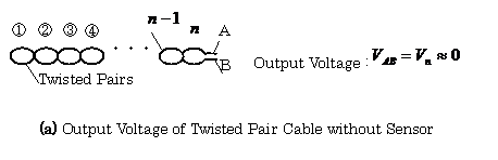
Fig.2.44
Twisted Cable for Sensor
[Chapter 3
will be presented in the upcoming January-February 2010 issue of this Journal.]
[ BWW Society Home Page ]
© 2009 The Bibliotheque: World Wide Society